Datasheet Texas Instruments SN74LVTH126 — Datenblatt
| Hersteller | Texas Instruments |
| Serie | SN74LVTH126 |
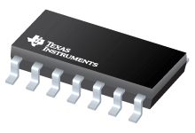
3,3-V-ABT-Vierfachbuspuffer mit 3-Zustands-Ausgängen
Datenblätter
SN54LVTH126, SN74LVTH126 datasheet
PDF, 722 Kb, Revision: B, Datei veröffentlicht: Oct 10, 2003
Auszug aus dem Dokument
Preise
Status
| SN74LVTH126D | SN74LVTH126DBR | SN74LVTH126DGVR | SN74LVTH126DR | SN74LVTH126DRG4 | SN74LVTH126NSR | SN74LVTH126PW | SN74LVTH126PWG4 | SN74LVTH126PWR | SN74LVTH126PWRE4 | SN74LVTH126PWRG4 | |
|---|---|---|---|---|---|---|---|---|---|---|---|
| Lifecycle Status | Active (Recommended for new designs) | Active (Recommended for new designs) | Active (Recommended for new designs) | Active (Recommended for new designs) | Active (Recommended for new designs) | Active (Recommended for new designs) | Active (Recommended for new designs) | Active (Recommended for new designs) | Active (Recommended for new designs) | Active (Recommended for new designs) | Active (Recommended for new designs) |
| Manufacture's Sample Availability | No | No | No | No | No | No | No | No | No | No | No |
Verpackung
| SN74LVTH126D | SN74LVTH126DBR | SN74LVTH126DGVR | SN74LVTH126DR | SN74LVTH126DRG4 | SN74LVTH126NSR | SN74LVTH126PW | SN74LVTH126PWG4 | SN74LVTH126PWR | SN74LVTH126PWRE4 | SN74LVTH126PWRG4 | |
|---|---|---|---|---|---|---|---|---|---|---|---|
| N | 1 | 2 | 3 | 4 | 5 | 6 | 7 | 8 | 9 | 10 | 11 |
| Pin | 14 | 14 | 14 | 14 | 14 | 14 | 14 | 14 | 14 | 14 | 14 |
| Package Type | D | DB | DGV | D | D | NS | PW | PW | PW | PW | PW |
| Industry STD Term | SOIC | SSOP | TVSOP | SOIC | SOIC | SOP | TSSOP | TSSOP | TSSOP | TSSOP | TSSOP |
| JEDEC Code | R-PDSO-G | R-PDSO-G | R-PDSO-G | R-PDSO-G | R-PDSO-G | R-PDSO-G | R-PDSO-G | R-PDSO-G | R-PDSO-G | R-PDSO-G | R-PDSO-G |
| Package QTY | 50 | 2000 | 2000 | 2500 | 2500 | 2000 | 90 | 90 | 2000 | 2000 | 2000 |
| Carrier | TUBE | LARGE T&R | LARGE T&R | LARGE T&R | LARGE T&R | LARGE T&R | TUBE | TUBE | LARGE T&R | LARGE T&R | LARGE T&R |
| Device Marking | LVTH126 | LXH126 | LXH126 | LVTH126 | LVTH126 | LVTH126 | LXH126 | LXH126 | LXH126 | LXH126 | LXH126 |
| Width (mm) | 3.91 | 5.3 | 4.4 | 3.91 | 3.91 | 5.3 | 4.4 | 4.4 | 4.4 | 4.4 | 4.4 |
| Length (mm) | 8.65 | 6.2 | 3.6 | 8.65 | 8.65 | 10.3 | 5 | 5 | 5 | 5 | 5 |
| Thickness (mm) | 1.58 | 1.95 | 1.05 | 1.58 | 1.58 | 1.95 | 1 | 1 | 1 | 1 | 1 |
| Pitch (mm) | 1.27 | .65 | .4 | 1.27 | 1.27 | 1.27 | .65 | .65 | .65 | .65 | .65 |
| Max Height (mm) | 1.75 | 2 | 1.2 | 1.75 | 1.75 | 2 | 1.2 | 1.2 | 1.2 | 1.2 | 1.2 |
| Mechanical Data | Herunterladen | Herunterladen | Herunterladen | Herunterladen | Herunterladen | Herunterladen | Herunterladen | Herunterladen | Herunterladen | Herunterladen | Herunterladen |
Parameter
| Parameters / Models | SN74LVTH126D | SN74LVTH126DBR | SN74LVTH126DGVR | SN74LVTH126DR | SN74LVTH126DRG4 | SN74LVTH126NSR | SN74LVTH126PW | SN74LVTH126PWG4 | SN74LVTH126PWR | SN74LVTH126PWRE4 | SN74LVTH126PWRG4 |
|---|---|---|---|---|---|---|---|---|---|---|---|
| Bits | 4 | 4 | 4 | 4 | 4 | 4 | 4 | 4 | 4 | 4 | 4 |
| F @ Nom Voltage(Max), Mhz | 160 | 160 | 160 | 160 | 160 | 160 | 160 | 160 | 160 | 160 | 160 |
| ICC @ Nom Voltage(Max), mA | 0.007 | 0.007 | 0.007 | 0.007 | 0.007 | 0.007 | 0.007 | 0.007 | 0.007 | 0.007 | 0.007 |
| Operating Temperature Range, C | -40 to 85 | -40 to 85 | -40 to 85 | -40 to 85 | -40 to 85 | -40 to 85 | -40 to 85 | -40 to 85 | -40 to 85 | -40 to 85 | -40 to 85 |
| Output Drive (IOL/IOH)(Max), mA | -32/64 | -32/64 | -32/64 | -32/64 | -32/64 | -32/64 | -32/64 | -32/64 | -32/64 | -32/64 | -32/64 |
| Package Group | SOIC | SSOP | TVSOP | SOIC | SOIC | SO | TSSOP | TSSOP | TSSOP | TSSOP | TSSOP |
| Package Size: mm2:W x L, PKG | 14SOIC: 52 mm2: 6 x 8.65(SOIC) | 14SSOP: 48 mm2: 7.8 x 6.2(SSOP) | 14TVSOP: 23 mm2: 6.4 x 3.6(TVSOP) | 14SOIC: 52 mm2: 6 x 8.65(SOIC) | 14SOIC: 52 mm2: 6 x 8.65(SOIC) | 14SO: 80 mm2: 7.8 x 10.2(SO) | 14TSSOP: 32 mm2: 6.4 x 5(TSSOP) | 14TSSOP: 32 mm2: 6.4 x 5(TSSOP) | 14TSSOP: 32 mm2: 6.4 x 5(TSSOP) | 14TSSOP: 32 mm2: 6.4 x 5(TSSOP) | 14TSSOP: 32 mm2: 6.4 x 5(TSSOP) |
| Rating | Catalog | Catalog | Catalog | Catalog | Catalog | Catalog | Catalog | Catalog | Catalog | Catalog | Catalog |
| Schmitt Trigger | No | No | No | No | No | No | No | No | No | No | No |
| Technology Family | LVT | LVT | LVT | LVT | LVT | LVT | LVT | LVT | LVT | LVT | LVT |
| VCC(Max), V | 3.6 | 3.6 | 3.6 | 3.6 | 3.6 | 3.6 | 3.6 | 3.6 | 3.6 | 3.6 | 3.6 |
| VCC(Min), V | 2.7 | 2.7 | 2.7 | 2.7 | 2.7 | 2.7 | 2.7 | 2.7 | 2.7 | 2.7 | 2.7 |
| Voltage(Nom), V | 3.3 | 3.3 | 3.3 | 3.3 | 3.3 | 3.3 | 3.3 | 3.3 | 3.3 | 3.3 | 3.3 |
| tpd @ Nom Voltage(Max), ns | 3.9 | 3.9 | 3.9 | 3.9 | 3.9 | 3.9 | 3.9 | 3.9 | 3.9 | 3.9 | 3.9 |
Öko-Plan
| SN74LVTH126D | SN74LVTH126DBR | SN74LVTH126DGVR | SN74LVTH126DR | SN74LVTH126DRG4 | SN74LVTH126NSR | SN74LVTH126PW | SN74LVTH126PWG4 | SN74LVTH126PWR | SN74LVTH126PWRE4 | SN74LVTH126PWRG4 | |
|---|---|---|---|---|---|---|---|---|---|---|---|
| RoHS | Compliant | Compliant | Compliant | Compliant | Compliant | Compliant | Compliant | Compliant | Compliant | Compliant | Compliant |
Anwendungshinweise
- LVT Family Characteristics (Rev. A)PDF, 98 Kb, Revision: A, Datei veröffentlicht: Mar 1, 1998
To address the need for a complete low-voltage interface solution, Texas Instruments has developed a new generation of logic devices capable of mixed-mode operation. The LVT series relies on a state-of-the-art submicron BiCMOS process to provide up to a 90% reduction in static power dissipation over ABT. LVT devices solve the system need for a transparent seam between the low-voltage and 5-V secti - LVT-to-LVTH ConversionPDF, 84 Kb, Datei veröffentlicht: Dec 8, 1998
Original LVT devices that have bus hold have been redesigned to add the High-Impedance State During Power Up and Power Down feature. Additional devices with and without bus hold have been added to the LVT product line. Design guidelines and issues related to the bus-hold features, switching characteristics, and timing requirements are discussed. - Bus-Hold CircuitPDF, 418 Kb, Datei veröffentlicht: Feb 5, 2001
When designing systems that include CMOS devices, designers must pay special attention to the operating condition in which all of the bus drivers are in an inactive, high-impedance condition (3-state). Unless special measures are taken, this condition can lead to undefined levels and, thus, to a significant increase in the device?s power dissipation. In extreme cases, this leads to oscillation of
Modellreihe
Serie: SN74LVTH126 (11)
Herstellerklassifikation
- Semiconductors> Logic> Buffer/Driver/Transceiver> Non-Inverting Buffer/Driver