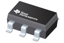
Datasheet Texas Instruments SN74LVC1G11-EP — Datenblatt
| Hersteller | Texas Instruments |
| Serie | SN74LVC1G11-EP |

Enhanced Product Single 3-Input Positive AND Gate
Datenblätter
Single 3-Input Positive AND Gate datasheet
PDF, 830 Kb, Datei veröffentlicht: Jul 17, 2009
Auszug aus dem Dokument
Preise
Status
| SN74LVC1G11MDCKREP | V62/09621-01XE | |
|---|---|---|
| Lifecycle Status | Active (Recommended for new designs) | Active (Recommended for new designs) |
| Manufacture's Sample Availability | Yes | Yes |
Verpackung
| SN74LVC1G11MDCKREP | V62/09621-01XE | |
|---|---|---|
| N | 1 | 2 |
| Pin | 6 | 6 |
| Package Type | DCK | DCK |
| Industry STD Term | SOT-SC70 | SOT-SC70 |
| JEDEC Code | R-PDSO-G | R-PDSO-G |
| Package QTY | 3000 | 3000 |
| Carrier | LARGE T&R | LARGE T&R |
| Device Marking | OBF | OBF |
| Width (mm) | 1.25 | 1.25 |
| Length (mm) | 2 | 2 |
| Thickness (mm) | .9 | .9 |
| Pitch (mm) | .65 | .65 |
| Max Height (mm) | 1.1 | 1.1 |
| Mechanical Data | Herunterladen | Herunterladen |
Parameter
| Parameters / Models | SN74LVC1G11MDCKREP | V62/09621-01XE |
|---|---|---|
| 3-State Output | No | No |
| Bits | 1 | 1 |
| F @ Nom Voltage(Max), Mhz | 150 | 150 |
| Gate Type | AND | AND |
| ICC @ Nom Voltage(Max), mA | 0.01 | 0.01 |
| Input Type | CMOS/TTL | CMOS/TTL |
| Logic | True | True |
| Operating Temperature Range, C | -55 to 125 | -55 to 125 |
| Output Drive (IOL/IOH)(Max), mA | 32/-32 | 32/-32 |
| Output Type | CMOS | CMOS |
| Package Group | SC70 | SC70 |
| Package Size: mm2:W x L, PKG | 6SC70: 4 mm2: 2.1 x 2(SC70) | 6SC70: 4 mm2: 2.1 x 2(SC70) |
| Rating | HiRel Enhanced Product | HiRel Enhanced Product |
| Schmitt Trigger | No | No |
| Sub-Family | AND Gate | AND Gate |
| Technology Family | LVC | LVC |
| VCC(Max), V | 5.5 | 5.5 |
| VCC(Min), V | 1.65 | 1.65 |
| Voltage(Nom), V | 1.8,2.5,3.3,5 | 1.8,2.5,3.3,5 |
| tpd @ Nom Voltage(Max), ns | 17.2,7.5,5.9,5 | 17.2,7.5,5.9,5 |
Öko-Plan
| SN74LVC1G11MDCKREP | V62/09621-01XE | |
|---|---|---|
| RoHS | Compliant | Compliant |
Anwendungshinweise
- LVC Characterization InformationPDF, 114 Kb, Datei veröffentlicht: Dec 1, 1996
This document provides characterization information about low-voltage logic (LVL) that operates from a 3.3-V power supply. It addresses the issues of interfacing to 5-V logic ac performance power considerations input and output characteristics and signal integrity for this family of devices. - Use of the CMOS Unbuffered Inverter in Oscillator CircuitsPDF, 796 Kb, Datei veröffentlicht: Nov 6, 2003
CMOS devices have a high input impedance high gain and high bandwidth. These characteristics are similar to ideal amplifier characteristics and hence a CMOS buffer or inverter can be used in an oscillator circuit in conjunction with other passive components. Now CMOS oscillator circuits are widely used in high-speed applications because they are economical easy to use and take significantly
Modellreihe
Serie: SN74LVC1G11-EP (2)
Herstellerklassifikation
- Semiconductors> Space & High Reliability> Logic Products> Little Logic Products