Datasheet Texas Instruments SN74AHC1G04-Q1 — Datenblatt
| Hersteller | Texas Instruments |
| Serie | SN74AHC1G04-Q1 |
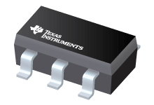
Automobilkatalog Single Inverter Gate
Datenblätter
Single Inverter Gate datasheet
PDF, 977 Kb, Revision: A, Datei veröffentlicht: Apr 15, 2008
Auszug aus dem Dokument
Preise
Status
| 1A1G04QDBVRG4Q1 | CAHC1G04QDCKRG4Q1 | SN74AHC1G04QDBVRQ1 | SN74AHC1G04QDCKRQ1 | |
|---|---|---|---|---|
| Lifecycle Status | Active (Recommended for new designs) | Active (Recommended for new designs) | Active (Recommended for new designs) | Active (Recommended for new designs) |
| Manufacture's Sample Availability | Yes | Yes | No | No |
Verpackung
| 1A1G04QDBVRG4Q1 | CAHC1G04QDCKRG4Q1 | SN74AHC1G04QDBVRQ1 | SN74AHC1G04QDCKRQ1 | |
|---|---|---|---|---|
| N | 1 | 2 | 3 | 4 |
| Pin | 5 | 5 | 5 | 5 |
| Package Type | DBV | DCK | DBV | DCK |
| Industry STD Term | SOT-23 | SOT-SC70 | SOT-23 | SOT-SC70 |
| JEDEC Code | R-PDSO-G | R-PDSO-G | R-PDSO-G | R-PDSO-G |
| Package QTY | 3000 | 3000 | 3000 | 3000 |
| Carrier | LARGE T&R | LARGE T&R | LARGE T&R | LARGE T&R |
| Device Marking | A04S | ACU | A04S | ACS |
| Width (mm) | 1.6 | 1.25 | 1.6 | 1.25 |
| Length (mm) | 2.9 | 2 | 2.9 | 2 |
| Thickness (mm) | 1.2 | .9 | 1.2 | .9 |
| Pitch (mm) | 0.95 | .65 | .95 | .65 |
| Max Height (mm) | 1.45 | 1.1 | 1.45 | 1.1 |
| Mechanical Data | Herunterladen | Herunterladen | Herunterladen | Herunterladen |
Parameter
| Parameters / Models | 1A1G04QDBVRG4Q1 | CAHC1G04QDCKRG4Q1 | SN74AHC1G04QDBVRQ1 | SN74AHC1G04QDCKRQ1 |
|---|---|---|---|---|
| 3-State Output | No | No | No | |
| Approx. price, US$ | .065 | 1ku | |||
| Bits | 1 | 1 | 1 | |
| F @ Nom Voltage(Max), Mhz | 75 | 75 | 75 | |
| Features | Balanced outputs,Very high speed (tpd 5-10ns),Over-voltage tolerant inputs | |||
| Gate Type | INVERTER BUFFER | INVERTER BUFFER | INVERTER BUFFER | |
| ICC @ Nom Voltage(Max), mA | 0.01 | 0.01 | 0.01 | |
| ICC(Max), uA | 10 | |||
| IOH(Max), mA | -8 | |||
| IOL(Max), mA | 8 | |||
| Input type | Standard CMOS | |||
| Logic | Inverting | Inverting | Inverting | |
| Number of channels | 1 | |||
| Operating Temperature Range, C | -40 to 125 | -40 to 125 | -40 to 125 | |
| Operating temperature range, C | -40 to 125 | |||
| Output Drive (IOL/IOH)(Max), mA | 8/-8 | 8/-8 | 8/-8 | |
| Output type | Push-Pull | |||
| Package Group | SC70|5,SOT-23|5 | SC70 | SOT-23 | SC70 |
| Package Size: mm2:W x L, PKG | 5SC70: 4 mm2: 2.1 x 2(SC70) | 5SOT-23: 8 mm2: 2.8 x 2.9(SOT-23) | 5SC70: 4 mm2: 2.1 x 2(SC70) | |
| Rating | Automotive | Automotive | Automotive | Automotive |
| Schmitt Trigger | No | No | No | |
| Special Features | Down translation to Vcc,low power | Down translation to Vcc,low power | Down translation to Vcc,low power | |
| Sub-Family | Inverting Buffer/Driver | Inverting Buffer/Driver | Inverting Buffer/Driver | |
| Supply voltage(Max), V | 5.5 | |||
| Supply voltage(Min), V | 2 | |||
| Technology Family | AHC | AHC | AHC | AHC |
| VCC(Max), V | 5.5 | 5.5 | 5.5 | |
| VCC(Min), V | 2 | 2 | 2 | |
| Voltage(Nom), V | 3.3,5 | 3.3,5 | 3.3,5 | |
| tpd @ Nom Voltage(Max), ns | 10.6,7.5 | 10.6,7.5 | 10.6,7.5 |
Öko-Plan
| 1A1G04QDBVRG4Q1 | CAHC1G04QDCKRG4Q1 | SN74AHC1G04QDBVRQ1 | SN74AHC1G04QDCKRQ1 | |
|---|---|---|---|---|
| RoHS | Compliant | Compliant | Compliant | Compliant |
| Pb Free | Yes |
Anwendungshinweise
- How to Select Little Logic (Rev. A)PDF, 1.1 Mb, Revision: A, Datei veröffentlicht: Jul 26, 2016
TI Little Logic devices are logic-gate devices assembled in a small single- dual- or triple- gate package. Little Logic devices are widely used in portable equipment such as mobile phones MP3 players and notebook computers. Little Logic devices also are used in desktop computers and telecommunications. Little Logic gates are common components for easy PC board routing schematic design and b - Migration From 3.3-V To 2.5-V Power Supplies For Logic DevicesPDF, 115 Kb, Datei veröffentlicht: Dec 1, 1997
This application report explores the possibilities for migrating to 3.3-V and 2.5-V power supplies and discusses the implications.Customers are successfully using a wide range of low-voltage 3.3-V logic devices. These devices are within Texas Instruments (TI) advanced low-voltage CMOS (ALVC) crossbar technology (CBT) crossbar technology with integrated diode (CBTD) low-voltage crossbar techn - Texas Instruments Little Logic Application ReportPDF, 359 Kb, Datei veröffentlicht: Nov 1, 2002
Portable and consumer electronic systems? needs present greater challenges today than ever before. Engineers strive to design smaller faster lower-cost systems to meet the market demand. Consequently the semiconductor industry faces a growing need to increase operating speed minimize power consumption and reduce packaging size. Texas Instruments manufactures a variety of Little Logic semicond - Benefits & Issues of Migrating 5-V and 3.3-V Logic to Lower-Voltage Supplies (Rev. A)PDF, 154 Kb, Revision: A, Datei veröffentlicht: Sep 8, 1999
In the last few years the trend toward reducing supply voltage (VCC) has continued as reflected in an additional specification of 2.5-V VCC for the AVC ALVT ALVC LVC LV and the CBTLV families.In this application report the different logic levels at VCC of 5 V 3.3 V 2.5 V and 1.8 V are compared. Within the report the possibilities for migration from 5-V logic and 3.3-V logic families - Advanced High-Speed CMOS (AHC) Logic Family (Rev. C)PDF, 102 Kb, Revision: C, Datei veröffentlicht: Dec 2, 2002
The Texas Instruments (TI) advanced high-speed CMOS (AHC) logic family provides a natural migration for high-speed CMOS (HCMOS) users who need more speed for low-power and low-drive applications. Unlike many other advanced logic families AHC does not have the drawbacks that come with higher speed e.g. higher signal noise and power consumption. The AHC logic family consists of gates medium-sca - Bus-Interface Devices With Output-Damping Resistors Or Reduced-Drive Outputs (Rev. A)PDF, 105 Kb, Revision: A, Datei veröffentlicht: Aug 1, 1997
The spectrum of bus-interface devices with damping resistors or balanced/light output drive currently offered by various logic vendors is confusing at best. Inconsistencies in naming conventions and methods used for implementation make it difficult to identify the best solution for a given application. This report attempts to clarify the issue by looking at several vendors? approaches and discussi - Selecting the Right Level Translation Solution (Rev. A)PDF, 313 Kb, Revision: A, Datei veröffentlicht: Jun 22, 2004
Supply voltages continue to migrate to lower nodes to support today's low-power high-performance applications. While some devices are capable of running at lower supply nodes others might not have this capability. To haveswitching compatibility between these devices the output of each driver must be compliant with the input of the receiver that it is driving. There are several level-translati - Live InsertionPDF, 150 Kb, Datei veröffentlicht: Oct 1, 1996
Many applications require the ability to exchange modules in electronic systems without removing the supply voltage from the module (live insertion). For example an electronic telephone exchange must always remain operational even during module maintenance and repair. To avoid damaging components additional circuitry modifications are necessary. This document describes in detail the phenomena tha - Introduction to LogicPDF, 93 Kb, Datei veröffentlicht: Apr 30, 2015
- Implications of Slow or Floating CMOS Inputs (Rev. D)PDF, 260 Kb, Revision: D, Datei veröffentlicht: Jun 23, 2016
- Understanding and Interpreting Standard-Logic Data Sheets (Rev. C)PDF, 614 Kb, Revision: C, Datei veröffentlicht: Dec 2, 2015
- Semiconductor Packing Material Electrostatic Discharge (ESD) ProtectionPDF, 337 Kb, Datei veröffentlicht: Jul 8, 2004
Forty-eight-pin TSSOP components that were packaged using Texas Instruments (TI) standard packing methodology were subjected to electrical discharges between 0.5 and 20 kV as generated by an IEC ESD simulator to determine the level of ISD protection provided by the packing materials. The testing included trays tape and reel and magazines. Additional units were subjected to the same discharge - TI IBIS File Creation Validation and Distribution ProcessesPDF, 380 Kb, Datei veröffentlicht: Aug 29, 2002
The Input/Output Buffer Information Specification (IBIS) also known as ANSI/EIA-656 has become widely accepted among electronic design automation (EDA) vendors semiconductor vendors and system designers as the format for digital electrical interface data. Because IBIS models do not reveal proprietary internal processes or architectural information semiconductor vendors? support for IBIS con - CMOS Power Consumption and CPD Calculation (Rev. B)PDF, 89 Kb, Revision: B, Datei veröffentlicht: Jun 1, 1997
Reduction of power consumption makes a device more reliable. The need for devices that consume a minimum amount of power was a major driving force behind the development of CMOS technologies. As a result CMOS devices are best known for low power consumption. However for minimizing the power requirements of a board or a system simply knowing that CMOS devices may use less power than equivale
Modellreihe
Serie: SN74AHC1G04-Q1 (4)
Herstellerklassifikation
- Semiconductors> Logic> Little Logic