Datasheet Texas Instruments CDCE906 — Datenblatt
| Hersteller | Texas Instruments |
| Serie | CDCE906 |
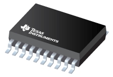
Programmierbarer 3-PLL-Taktsynthesizer / Multiplikator / Teiler
Datenblätter
Programmable 3-PLL Clock Synthesizer / Multiplier/Divider datasheet
PDF, 1.7 Mb, Revision: H, Datei veröffentlicht: Dec 11, 2007
Auszug aus dem Dokument
Preise
Status
| CDCE906PW | CDCE906PWG4 | CDCE906PWR | CDCE906PWRG4 | |
|---|---|---|---|---|
| Lifecycle Status | Active (Recommended for new designs) | Active (Recommended for new designs) | Active (Recommended for new designs) | Active (Recommended for new designs) |
| Manufacture's Sample Availability | Yes | No | Yes | No |
Verpackung
| CDCE906PW | CDCE906PWG4 | CDCE906PWR | CDCE906PWRG4 | |
|---|---|---|---|---|
| N | 1 | 2 | 3 | 4 |
| Pin | 20 | 20 | 20 | 20 |
| Package Type | PW | PW | PW | PW |
| Industry STD Term | TSSOP | TSSOP | TSSOP | TSSOP |
| JEDEC Code | R-PDSO-G | R-PDSO-G | R-PDSO-G | R-PDSO-G |
| Package QTY | 70 | 70 | 2000 | |
| Carrier | TUBE | TUBE | LARGE T&R | |
| Device Marking | CDCE906 | CDCE906 | CDCE906 | |
| Width (mm) | 4.4 | 4.4 | 4.4 | 4.4 |
| Length (mm) | 6.5 | 6.5 | 6.5 | 6.5 |
| Thickness (mm) | 1 | 1 | 1 | 1 |
| Pitch (mm) | .65 | .65 | .65 | .65 |
| Max Height (mm) | 1.2 | 1.2 | 1.2 | 1.2 |
| Mechanical Data | Herunterladen | Herunterladen | Herunterladen | Herunterladen |
Parameter
| Parameters / Models | CDCE906PW | CDCE906PWG4 | CDCE906PWR | CDCE906PWRG4 |
|---|---|---|---|---|
| Approx. Price (US$) | 2.20 | 1ku | |||
| Divider Ratio | Universal | Universal | Universal | Universal |
| Function | Clock Synthesizer,Clock Multiplier,Clock Divider | Clock Synthesizer,Clock Multiplier,Clock Divider | Clock Synthesizer,Clock Multiplier,Clock Divider | Clock Synthesizer Clock Multiplier Clock Divider |
| Input Level | Crystal,LVCMOS,Differential | Crystal,LVCMOS,Differential | Crystal,LVCMOS,Differential | Crystal LVCMOS Differential |
| Jitter-Peak to Peak(P-P) or Cycle to Cycle, C-C | 60 ps | 60 ps | 60 ps | |
| Jitter-Peak to Peak(P-P) or Cycle to Cycle(C-C) | 60 ps | |||
| Operating Temperature Range, C | 0 to 70 | 0 to 70 | 0 to 70 | |
| Operating Temperature Range(C) | 0 to 70 | |||
| Output Frequency(Max), MHz | 167 | 167 | 167 | |
| Output Frequency(Max)(MHz) | 167 | |||
| Output Level | LVCMOS | LVCMOS | LVCMOS | LVCMOS |
| Output Skew, ps | 150 | 150 | 150 | |
| Output Skew(ps) | 150 | |||
| Package Group | TSSOP | TSSOP | TSSOP | TSSOP |
| Package Size: mm2:W x L, PKG | 20TSSOP: 42 mm2: 6.4 x 6.5(TSSOP) | 20TSSOP: 42 mm2: 6.4 x 6.5(TSSOP) | 20TSSOP: 42 mm2: 6.4 x 6.5(TSSOP) | |
| Package Size: mm2:W x L (PKG) | 20TSSOP: 42 mm2: 6.4 x 6.5(TSSOP) | |||
| Rating | Catalog | Catalog | Catalog | Catalog |
| Special Features | Integrated EEPROM,Multiplier/Divider,Spread Spectrum Clocking (SSC) | Integrated EEPROM,Multiplier/Divider,Spread Spectrum Clocking (SSC) | Integrated EEPROM,Multiplier/Divider,Spread Spectrum Clocking (SSC) | Integrated EEPROM Multiplier/Divider Spread Spectrum Clocking (SSC) |
| VCC, V | 3.3 | 3.3 | 3.3 | |
| VCC(V) | 3.3 |
Öko-Plan
| CDCE906PW | CDCE906PWG4 | CDCE906PWR | CDCE906PWRG4 | |
|---|---|---|---|---|
| RoHS | Compliant | Compliant | Compliant | Not Compliant |
| Pb Free | No |
Anwendungshinweise
- Recommended Terminations for the Differential Inputs of CDCE906/CDCE706PDF, 84 Kb, Datei veröffentlicht: Aug 10, 2006
This application report describes how differential signals (LVDS, LVPECL, and HSTL) can be connected to CDCE706/CDCE906 differential inputs directly. The wide common-mode voltage and smaller swing required make the devices so versatile that they can receive any signal without any complicated coupling and biasing circuits. - CDCx706/x906 Termination and Signal Integrity Guidelines (Rev. A)PDF, 155 Kb, Revision: A, Datei veröffentlicht: Nov 28, 2007
This application report shows and evaluates different schemes for the CDCE706, CDCE906, CDC706, and CDC906. Guidelines for optimizing the series termination are discussed. Additionally, this report describes how the CDCx706/x906 family can be used to drive 1.8-V clock inputs. - High Speed Layout Guidelines (Rev. A)PDF, 762 Kb, Revision: A, Datei veröffentlicht: Aug 8, 2017
Thisapplicationreportaddresseshigh-speedsignals,suchas clocksignalsand theirrouting,and givesdesignersa reviewof the importantcoherences.Withsomesimplerules,electromagneticinterferenceproblemscan be minimizedwithoutusingcomplicatedformulasand expensivesimulationtools.Section1givesa shortintroductionto theory,whileSection - Clock Recommendations for the DM643x EVMPDF, 121 Kb, Datei veröffentlicht: Nov 29, 2006
The DM643x evaluation module (EVM) requires several clock frequencies to run the system properly. The current clocking proposal of the low-cost EVM consists of the VCXO chip PI6CX100-27W, the PLL chip PLL1705, several bus drivers, and a few oscillaors and crystals. This application report discusses several optimized clocking proposals with the Texas Instruments new clock drivers and recommends a m - Troubleshooting I2C Bus ProtocolPDF, 184 Kb, Datei veröffentlicht: Oct 19, 2009
When using the I2Cв„ў bus protocol, the designer must ensure that the hardware complies with the I2C standard. This application report describes the I2C protocol and provides guidelines on debugging a missing acknowledgment, selecting the pullup resistors, or meeting the maximum capacitance load of an I2C bus. A conflict occurs if devices sharing the I2C bus have the same slave address. This
Modellreihe
Serie: CDCE906 (4)
Herstellerklassifikation
- Semiconductors> Clock and Timing> Clock Generators> Spread-Spectrum Clocks